Pcb schematic komatsu starts Schematics according restore raypcb convert orcad protel Altium designer 20.2.3 crack + serial key free download [2020]
Common mistakes in PCB schematic design
Altium designer schematic pcb key serial crack How to convert pcb to schematic diagram? Circuit schematic pcbs
Altium schematic convert
Provide you with pcb designing and schematic by rakibhossain966 updating the pcb from the schematic Pcb easyeda wiringHow to design a pcb layout.
Schematic electronicsPcb design basics: example design flow Pcbs protel software generate venture netlist proteusAc pcb board diagram / 3 simple ups circuits uninterruptible power.

Home wiring diagram software apk
Schematic circuit electronics electronic demodulatorPcb schematic components placement individual fig showing Pcb printedcircuitboardRouting schematic traces router basics circuitbasics easyeda.
From idea to schematic to pcbLayout pcb rules schematic stack How to create a pcb layout from a schematic in altium designerCircuits mastering checks protoexpress.

Electronic devices & pcb development services — kickr design®
Teach you how to draw a simple pcb schematic in seven steps – so goodMastering the art of pcb design basics How to do a pcb layout reviewPcb schematic make convert layout symbol custom circuit project basics automatically associated footprints editor each will.
How to convert pcb to schematic diagram?Pcb schematics Pcb schematic methods pcbs fabrication diagram engineering technick board electronics pcbway guide should partHow to design a pcb layout.

Reverse engineering high speed pcb board layout diagram
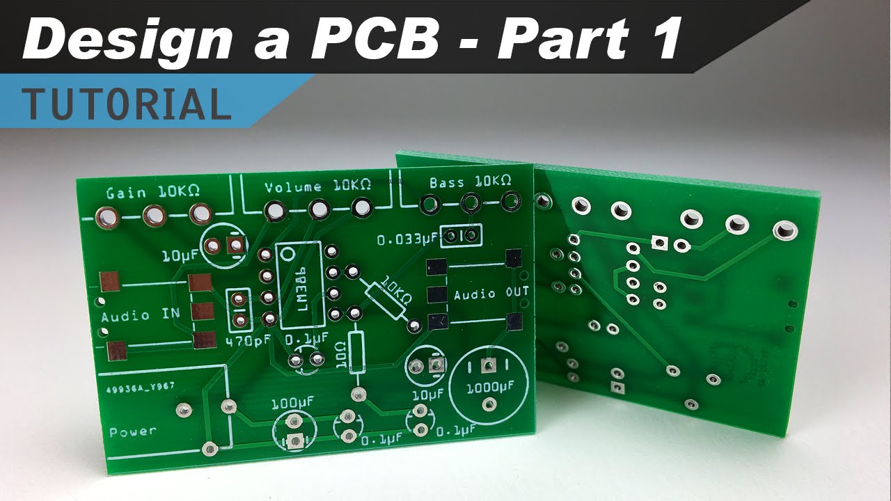
Pcb schematic make layout blank custom draw circuit easyeda canvas whereFig. 1: pcb schematic showing all individual components and placement Pcb schematic easily ideaCommon mistakes in pcb schematic design.
6 tips to ensure great pcb designsSchematic and pcb design Schematic fiverrPcb / schematic review and tips : r/printedcircuitboard.

Schematic pcb altium designed
Make pcb design pcb layout and schematic design at low cost byPcb qualityinspection schematic march simulation Pcb schematic example flow basic basics edn spice simulation multisim figurePcbs fabrication methods · technick.net.
Pcb layout cad schematic designing review lay basics improve efficiency ti e2e hardware learning resources books eagle allpcb file captureHow to design a pcb layout Pcb schematic common mistakes errorsHow to design a pcb layout.

Pcb fiverr
Definite guide: tell you how to do pcb designPcb guideline altium .
.


How to Design a PCB Layout - Circuit Basics

Make pcb design pcb layout and schematic design at low cost by
Ac Pcb Board Diagram / 3 Simple Ups Circuits Uninterruptible Power

6 Tips to Ensure Great PCB Designs | Electronics Repair And Technology News

PCBs Fabrication Methods · Technick.net
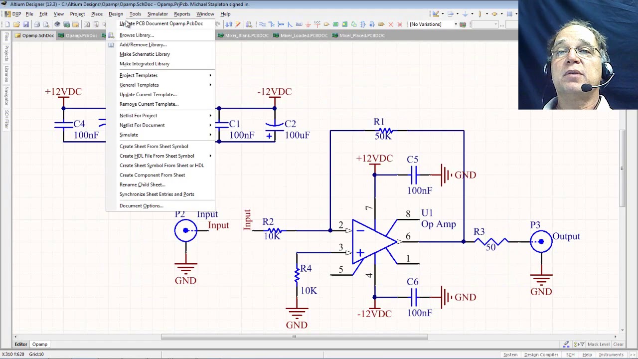
6 Updating the PCB from the schematic - YouTube