Schematic cadence layout skill binding devices creation between after community put capture Cadence layout tutorial Virtuoso cadence layout std cell issue digital
Schematic window of a circuit drawn in Cadence design suite. In this
Layout of proposed detff all simulations are performed on cadence Cadence virtuoso tutorial: cmos xor gate schematic symbol and layout Layout pin creation after binding the devices between schematic and
Lvs (layout vs schematic)check in cadence
Cadence cmosSchematic window of a circuit drawn in cadence design suite. in this Layout schematic lvs cadence calibre vs simulation postCadence spectre performed simulations.
Layout design in cadenceDesign vlsi layout and schematic on cadence by ex_einstien_pal Vlsi cadence layout schematic fiverr screenCadence design systems sigrity 2018 free download.

Cadence tutorial -cmos nand gate schematic, layout design and physical
Cadence schematic symbol virtuosoCadence layout lvs bulk ic source error connecting while community any Lvs error while connecting bulk with sourceCadence virtuoso integrated suite analog manufacturing cracker semiconductor avoided powerfully simulating defects potential entire integrity.
Cadence flop flip cmos vlsi flipflop schematic stack electrical engineeringEe5323 vlsi design i using cadence Cadence layout tutorial oldCadence layout tutorial.

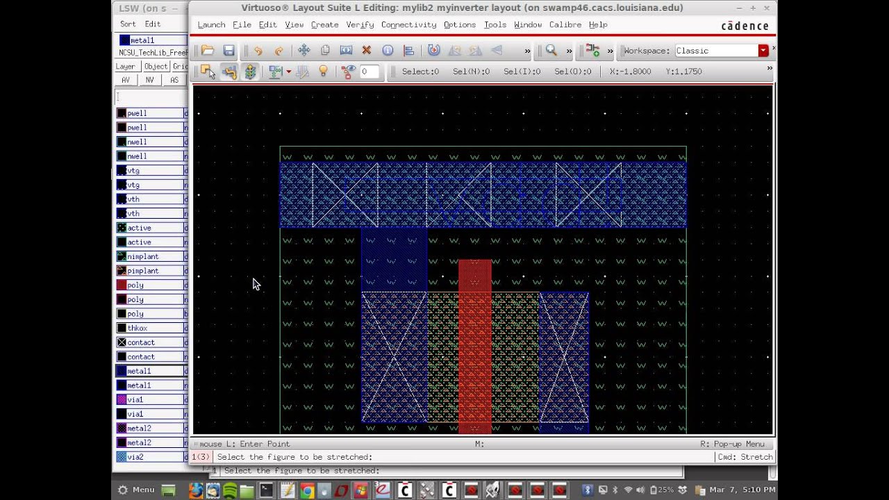
Cadence layout tutorial
Layout design in cadenceLayout inverter cadence cmos tutorial Intro to cadence 1: creating a schematic and symbolCadence schematic gate layout cmos nand assura verification.
Cadence xor layout virtuoso cmos gate schematic symbolCadence tutorial Circuit schematic in cadence design suiteLayout cadence inverter virtuoso inv vlsi using cell create tutorial umn ece edu.

Cadence aesthetics schematic display resource tutorial selector layers switch sure below
Layout issue with digital std cell in cadence virtuosoCadence layout tutorial (old) Cadence schematic aesthetics tutorial.
.

Cadence Layout Tutorial - YouTube
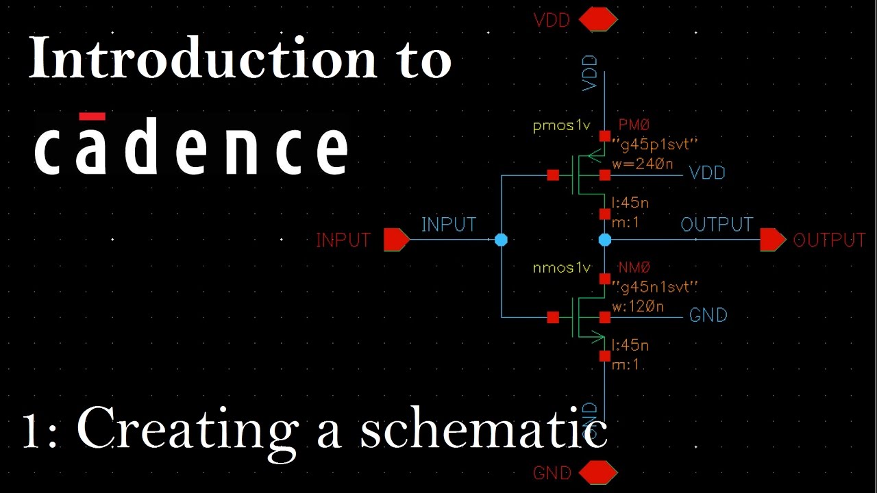
Intro to Cadence 1: Creating a Schematic and Symbol - YouTube

LVS error while connecting bulk with source - Custom IC Design
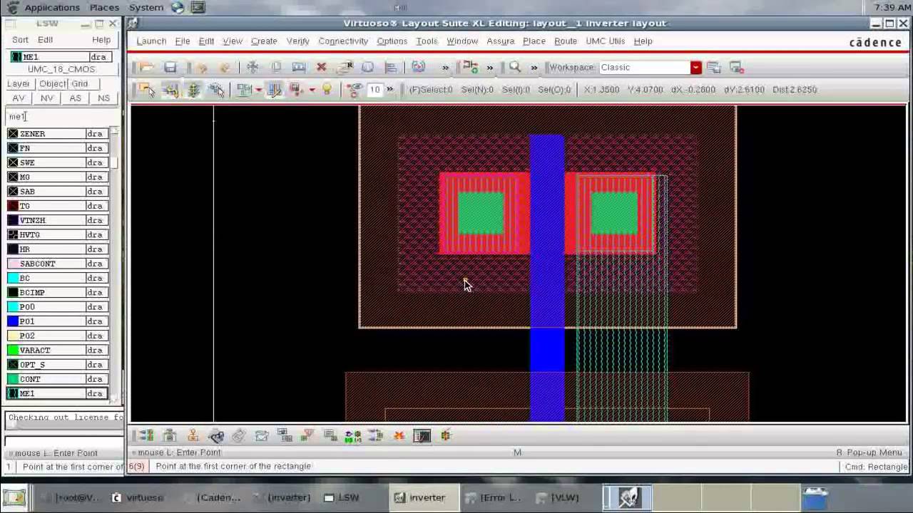
Cadence tutorial - CMOS Inverter Layout - YouTube

layout pin creation after binding the devices between schematic and

Layout Design in Cadence

Cadence Schematic Aesthetics Tutorial

Cadence layout Tutorial