Controlled impedance routing in altium designer Altium routing traces primitives 1 (schematic circuit using altium designer 2017) source: researcher
Controlled Impedance Routing in Altium Designer | Sierra Circuits
Schematic altium io checker symbols wired wiring designer Managing design changes between the schematic & the pcb in altium Altium impedance integrity signal differ dru pcb
Io checker: wiring schematic symbols
Altium circuit engineering schematic designer embedded system will dialog button clickAltium schematic researcher Altium entries sheet useTest point altium symbol schematic create footprint designer testing created updated november april.
Altium designer wiring diagramAltium pcb routing managing howie vault Altium schematic viewer designer software pcb editor diagram example open circuit comparison wiring document result viewing documents ultimate monitorEmbedded system engineering: altium designer tutorial 3.

Embedded system engineering: altium designer tutorial 3
Altium header pcb schematic example reset eevblog forum between thereSchematic altium pdk ops mismatch document between devzone specification sheet nordic Altium schematic circuit designer tutorial pcb component layout system embedded engineering will select menu place addDesign rule check altium drc.
How to create a test point schematic symbol and footprint in altiumPcb altium Newbie altium errorsSchematic mismatch between ops document and pdk schematic.


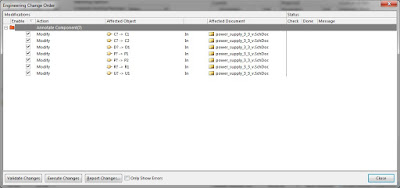
Managing Design Changes between the Schematic & the PCB in Altium
Embedded System Engineering: Altium Designer Tutorial 3 - Circuit Schematic

Design Rule Check Altium DRC - Part 2 [ Arduino PCB Design Course

Schematic mismatch between OPS document and PDK schematic - Nordic Q&A

schematics - Use sheet entries on Altium - Electrical Engineering Stack

1 (Schematic Circuit using Altium Designer 2017) Source: Researcher

pcb - Altium - Impedance in Signal Integrity and DRU differ

Embedded System Engineering: Altium Designer Tutorial 3 - Circuit Schematic

How to Create a Test Point Schematic Symbol and Footprint in Altium

Controlled Impedance Routing in Altium Designer | Sierra Circuits